Raman demystified

Most gemologists have some difficulties understanding FTIR, UV-VIS-NIR, LIBS, SIMS, LA-ICP-MS and other advanced alphabet soup techniques used in modern gemological laboratories.

Raman is different - from gemologist's point of view it really doesn't differ much from classical crossed filters technique. Sample is excited with monochromatic light source and the spectrum exhibits "emission lines" at higher wavelengths just like studying fluorescence. These Raman peaks constitute a diagnostic fingerprint for material identification. The only problem is the inherent weakness of the Raman effect. Traditional spectroscope and human eye can't see the lines no matter how hard you try.

It's almost 100 years old technology!

Don't worry; we are not going too deep in to physics. With Raman you can do it later and we promise there is no limits to the complexity of the subject. Instead, now we are trying to limit the information to that any trained gemologist can follow.

The Raman scattering effect of light is all but prime time news - it was first theorized almost 100 years ago. It was first demonstrated 1928 by Indian scientist C.V. Raman who later received Nobel prize in physics for his discovery. He was also knighted by the British Government in 1929 and became director of the Indian Institute of Science.

Here is what was found. When light traverses a transparent material, some of the light that is scattered changes in color aka. wavelength. 

Unlike light scattering at crystal borders or inclusions of some materials known by gemologists, the Raman effect is related to vibrations of atomic bonds. Therefore it happens in perfectly flawless transparent materials too.

Most of the light scattering happens at same wavelength as the excitation source. In this case the incoming ray just changes its direction of propagation. This effect is called Rayleigh scattering and it does not contain any information about the material under study. About 1 out of one million photons interact with molecular bonds, causing its wavelength to shift up or down. Shifting up to longer wavelength is stronger and it is called Stokes shift. Each chemical bond between atoms creates certain shifts according to complicated rules.

Raman spectrum

To get started you don't have to get involved with the scattering rules. Your job (or actually your computer's job) is to interpret the spectral information and refer it against established spectral library of known materials. Without a reference library the Raman spectra are just a set of wiggly lines.

Raman shift is too weak effect to be observed by bare eyes. High sensitivity digital spectrometer is needed to resolve the "emission lines" instead of a traditional spectroscope.

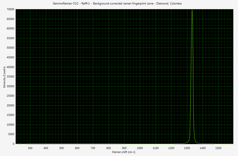
On the right side you can see Raman spectrum of colorless diamond recorded with digital spectrometer. Please click the image to see it in full size. The x-axis of spectrum contains the wavelength information (don't let cm-1 units to bother your, these are discussed later) and y axis is the intensity of light.

The diamond Raman peak produced by sp3 bonding between carbon atoms is located at 1332 cm-1. The excitation source in this case was monochromatic 532 nm (green) laser. The source has to be monochromatic and powerful enough to create detectable amount of shifted photons. In real life laser is the only light source fulfilling these requirements.

Photoluminescence (PL)

The person operating a Raman spectrometer should be aware of photoluminescence reactions such as fluorescence. That's right, fluorescence reactions are not only privilege of UV light sources but also occur often with visible light sources too. 

This effect between interaction of photons and electrons is often present when Raman spectrum is recorded. The problem is that fluorescence may be 1000 times stronger than Raman signal and mask it totally.

On the right you see a sample spectrum of sinhalite. Again, please click the image for seeing it in full size. Weak Raman peaks can be seen on the left corner of the spectrum. The much larger signal at the right corner of the spectrum comes from luminescence.

When studying gemological materials, luminescence may reveal additional information and helps to identify chromophores or defects in crystal lattice. Sometimes it helps to identify material at first sight as in the case of sinhalite. It should be noted interpreting PL signals is often much more complicated than Raman and requires experience or good reference.

Lasers

Power levels of the typical lasers used in Raman spectroscopy are in the range of 10-500mW. That is more than enough to cause damage if collimated beam hits the retina of an eye. If a Raman setup has not been built to be completely safe (as we do) you must use protective eyewear! A mistake blinds you or another person in the room - you have been warned!

The most common wavelengths of lasers used for Raman spectroscopy are 785nm diode laser at infrared and 532nm DPSS laser at green. In theory the wavelength of laser should not change amount of shift from original wavelength.

Photoluminescence reactions like fluorescence are often considered as spectral artifacts (flaws) by Raman scientists. As these effects are rarer when IR excitation is used, a 785nm laser is traditional choice for Raman spectroscopy. However, green laser produces Raman effect 5 times more efficiently than IR wavelength. We have elected to use a 532nm laser in our GemmoRaman-532 product and online database. Online reference for minerals is available for both lasers (RRUFF Project).


Why nanometers are not used in Raman spectroscopy?

Gemologists have been taught to use nanometers as wavelength unit for visible light spectroscopy. However, another unit - wavenumber has been in use for IR spectroscopy since the 1950's. Wavenumber is expressed in the reciprocal centimeter (cm-1) units, and is proportional to the energy of the photon. Wavenumber simply tells the count of waves per centimeter. True relationship between wavenumber and energy level was the reason IR spectroscopists decided to use cm-1 instead of nanometers.

Raman scattering and infrared absorption are both consequence of vibration of atomic bondings. Each atomic bond vibration type is either Raman active or IR-active, so that the resulting spectra do not look similar. As these techniques are complementary, scientists have adopted the usage of cm-1 as Raman shift unit.

Raman shift unit does not indicate the actual energy of the emission but how far it is shifted from the excitation source (laser) energy. This shift - if expressed as wavenumbers - is always the same no matter what excitation wavelength has been used.

Example: If a diamond is excited with 532 nm laser it will show Raman peak at about 573 nm. Raman shift expressed in nanometers is simple subtraction between the two wavelengths = 41nm.  If same diamond is excited with 405 nm blue laser the Raman peak exists at 428 nm. Raman shift in nanometers in this case is only 23 nm. If we translate all the used wavelengths to wavenumbers before subtraction we will notice the Raman shift is 1332 cm-1 in both cases.

Miniature spectrometers

With the invention of miniature spectrometer, OceanOptics has revolutionized spectroscopy applications since the 1990's. The asymmetrical crossed Czerny-Turner optical bench has no moving parts, which results in a robust system with extremely good repeatability. Miniature spectrometer is relatively low cost analytical instrument compared to scanning spectrometers, which has dominated Raman spectroscopy for decades. CCD (Charge Coupled Device) type spectrometer contains a row of thousands of photo-sensitive pixels similar to digital cameras. Incoming light is dispersed to the CCD sensor via diffraction grating.

A CCD-Spectrometer is essentially a digital version of diffraction grating spectroscope. Instead of the picture of the spectrum it plots the light intensity at different wavelengths to 2-dimensional graphic presentation. CCD sensors are much more sensitive than human eye and can detect wavelengths between 200 and 1100nm. In other words the wavelength scale is extended to both UV and IR directions compared to spectroscope.

Typical Raman shifts of visible wavelength monochromatic light are in the range of 10-150nm. A spectrometer dedicated to Raman application does not have to cover the whole range from UV to IR. Instead, its range is adjusted to start right after the wavelength of selected laser source and to stop at 100-200nm higher wavelength. For example, GemmoRaman-532™ has a spectrometer whose wavelength scale covers the region between 535-700nm, i.e., the green, yellow, orange and red areas of visible light spectrum.

How to read Raman spectra

A Raman spectrum contains information about photons that are shifted relative to the excitation source. The x- axis does not indicate actual wavenumber (or wavelength) of light but amount of the shift from original laser wavenumber. Laser wavelength is plotted on the left or the right side of the scale and it is located at 0 cm-1. There is no Raman spectrometer capable of plotting Raman shift right after zero. Spectrometers ability to record low shift wavenumbers depends on the filtration of the laser photons. That is why Raman spectrum typically starts from somewhere between 60 and 350 cm-1.

The area from 0 to about 1600 cm-1 is the so-called Raman “fingerprint zone”. The spectral pattern of this area reflects a fingerprint enabling the identification of a material, just as a fingerprint enables the identification of a person. This is also the area in which most Raman signals of inorganic solids occur. Many times you will see a spectrum recorded only across fingerprint zone. Usually that means there was no gemologically relevant information at higher wavenumbers. Fingerprint spectra are also typically background corrected. This means any slope generated by luminescence has been subtracted from the spectrum. Background correction prepares the data for the computer to find the peak locations and match them against a library containing spectra of known materials.

The extended area form 0 to about 3000-6000 cm-1 (depending on spectrometer) is called a “broad scan area”. Broad scan contains both Raman fingerprint zone and a extended range for photoluminescence studies. The line between the zones is not very distinct. Photoluminescence reactions do occur at both areas and sometimes mix with or overwhelm any Raman signals. Another typical scene is small Raman peaks riding on top of broad and intense luminescence line. For gemology it is advisable to pay attention to luminescence as much as Raman signals, because it often contains important information about chromophores (such Cr) and rare earth elements (REE).

Importance of spectrometer resolution

Spectrometer's resolution defines its ability to resolve two adjacent wavelengths so that they can be separated from each other. Typical resolution of a CCD-type UV-VIS-NIR spectrometer having range 300-800nm is about 1nm (30cm-1). This could be considered a minimum requirement for Raman spectrometer in gemology. Better results can be obtained if both resolution and wavelength range of the spectrometer is optimized for the selected laser wavelength.

We are publishing 0.3nm (10cm-1) resolution spectra in our libraries because it is the most convenient resolution allowing both material identification by Raman fingerprint and extended range for photoluminescence studies. This is also the resolution we have elected for use in our dual purpose (Raman/PL) GemmoRaman-532™ product. Even better resolutions can be achieved with more costs and reduced scale if only Raman fingerprint zone is of interest. However, the natural peak width of solid inorganic materials is about 6 cm-1 and so more resolution gives only very small benefits compared to price tag of narrower wavelength laser and higher resolution spectrometer.

Gemologists work with relatively limited amount of materials compared to chemists and geologists. While 0.3nm (10cm-1) spectrometer does not resolute all the peaks of materials it is still very powerful tool for gem identification. The key skill in spectra interpretation is to learn how to see "overlapping peaks" by looking for deviations in peak formation. These deviations show up usually so that a peak does not follow nice Gaussian distribution.

On the right you see Raman spectra of demantoid garnet sample recorded with spectrometers having resolution of 1 nm (green line) and 0.3 nm resolution (white line). With good imagination almost all the peaks of better resolution white line can be "seen" in lower resolution green line.

Computers are perfect in finding best match from the library if resolutions of both sample and library are about the same. Unfortunately computers are not so good in imagination. If the resolution of the sample spectrum differs a lot from library entries the computer is not able to find the match.

Laser blocking filters

One of the most important parts in Raman probe is a device which is able to remove the laser wavelength photons completely from signal before it is guided to the spectrometer. Remember only 1 out of million photons was ever Raman shifted? Too much laser light saturates (overexposure) the CCD of the spectrometer and leaks to the adjacent pixels making Raman peaks unreadable.

Removing laser light is another reason why high end Raman spectrometers cost more than a new high-end car. The typical method is to use not only one but three or more diffraction gratings or prisms for separating the laser wavelength more precisely. Recent development in manufacturing of interference filters have simplified Raman spectrometer operation and reduced the costs. These filters have very distinct "edge" - a wavelength where total blocking of light turns to transmission. The best filters are able to block all laser light but pass everything just a couple nanometers beyond.